Success in 3D integration of analog ICs OKI and Nisshinbo

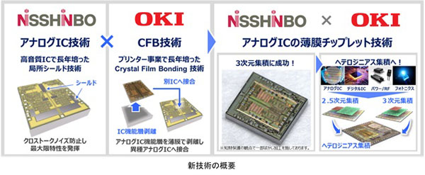
OKI, in collaboration with Nisshinbo Microdevices, has succeeded in 3D integration of thin-film analog ICs using CFB (Crystal Film Bonding) technology.
CFB is OKI’s proprietary technology that peels off the functional layer of a semiconductor device and bonds it to a substrate of a different material using intermolecular forces.
This technology can be applied to the integration of various semiconductor devices such as analog ICs. The two companies are aiming for mass production in 2026.
As semiconductor needs increase, attention is being paid to chiplet technology, which achieves large-scale functional integration at low cost and in a small area by dividing each function into small chips and integrating them using 2D, 5D, and 3D mounting technology, rather than integrating all functions into a single chip.
In order to apply chiplet technology to the 3D integration of low-end analog ICs, several issues must be resolved, such as cost and the prevention of noise (crosstalk noise) caused by interference of electrical signals.
To resolve the cost issue, OKI developed “thin-film chiplet technology.” Thin-film chiplet technology consists of a CFB process for peeling and bonding, followed by rewiring. Because the thin-film analog ICs bonded using this technology are extremely thin, it is possible to apply common, inexpensive legacy processes for rewiring.
Thin-film chiplet technology can be applied to the integration of a variety of semiconductor devices, including digital, analog, optical, power, and sensor devices. OKI hopes that this will lead to new advances in semiconductor devices.
To prevent noise, Nisshinbo Micro Devices applied its unique local shielding technology to analog ICs. By applying shielding only to specific locations that are affected between the upper and lower chips, it has succeeded in suppressing signal interference without compromising circuit function.
※Translating Japanese articles into English with AI
